
什么是抖动,为什么它很重要?
Contents
- Introduction
- Defining Jitter and Phase Noise
- Jitter and Phase Noise Impact on Audio Converters
- Conclusion
Introduction
An audio system’s performance depends on the characteristics of its elements (such as converters, amplifiers, or transducers) and the environmental conditions that it is operating under (such as temperature, supply noise, or EMI).
A low-quality clock signal can be a performance-limiting factor, even if the other elements in the system deliver a high-quality performance. Therefore, it is vital to consider the quality of the clock signal when designing the system.
The clock is the heartbeat of the system, and its accuracy, precision, and stability are significant design considerations.
Defining Jitter and Phase Noise
Jitter
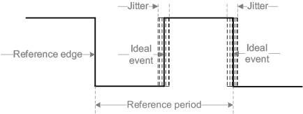
Jitter refers to the general concept of clocking precision error and is defined as “the dynamic deviation of event instants in a stream or signal from their ideal position in time, excluding modulation components below 10 Hz.”1
There are various types of jitter, each measured differently, and applications vary in their sensitivity to different types. The two fundamental types of jitter are absolute jitter and N-period jitter. These are quantified as:
-
Absolute jitter: Deviation of the clock edge position from an ideal clock used as reference.
-
N-period jitter: Deviation in cycle duration from the ideal period, measured over a specified number (N) of consecutive periods. Period jitter is N-period jitter, where N = 1.
Period jitter is the derivative of absolute jitter. Furthermore, absolute jitter is the accumulation of period jitter. Therefore, we can measure one of the two and derive mathematically the other.
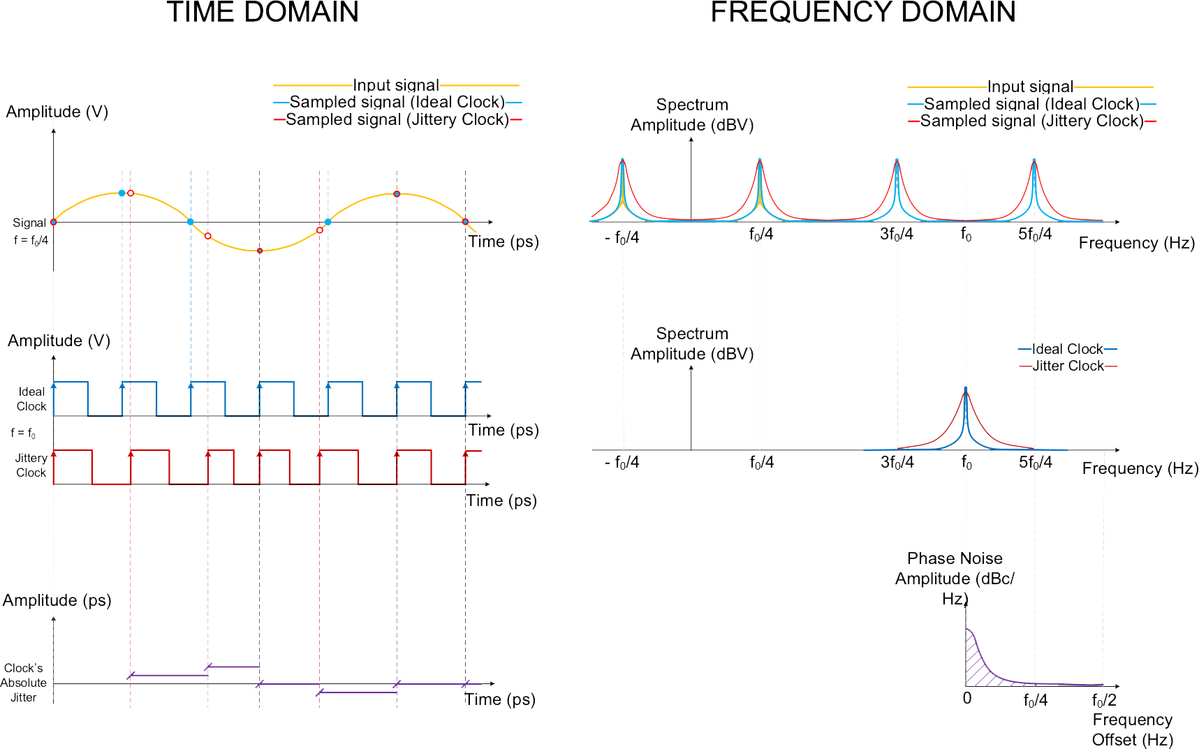
Absolute and period jitter resulting from a non-ideal clock signal are shown in Figure 1.
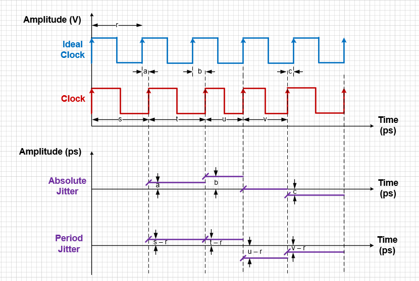
Deviations in the clock edge or the period, with respect to the ideal clock, result in an equivalent absolute jitter or period jitter amplitude respectively. The resulting jitter persists for a single clock cycle duration.
For example, in Figure 1, during the first clock cycle, the rising edge of the clock deviates from the rising edge of the ideal clock by a picoseconds. This is shown as an amplitude of a picoseconds of absolute jitter. Similarly, in the first clock cycle, the period of the clock, s, deviates from the period of the ideal clock by s – r picoseconds. This is shown as an amplitude of s – r picoseconds of period jitter. Note that absolute and period jitter can be negative if the rising edge of the clock rises before the rising edge of the ideal clock, or if the period of the clock is less than the period of the ideal clock, as demonstrated in the fifth clock cycle in Figure 1.
Jitter is a time domain measurement of clock precision error. In the frequency domain, clock precision error is characterized by phase noise analysis. Frequency domain analysis is useful in audio applications, as sensitivity to jitter in an audio converter is frequency dependent.
Phase Noise
Phase noise describes the spectral distribution of jitter. A plot of phase-noise amplitude against frequency offset, where f0 is the clock frequency, is shown in Figure 2.
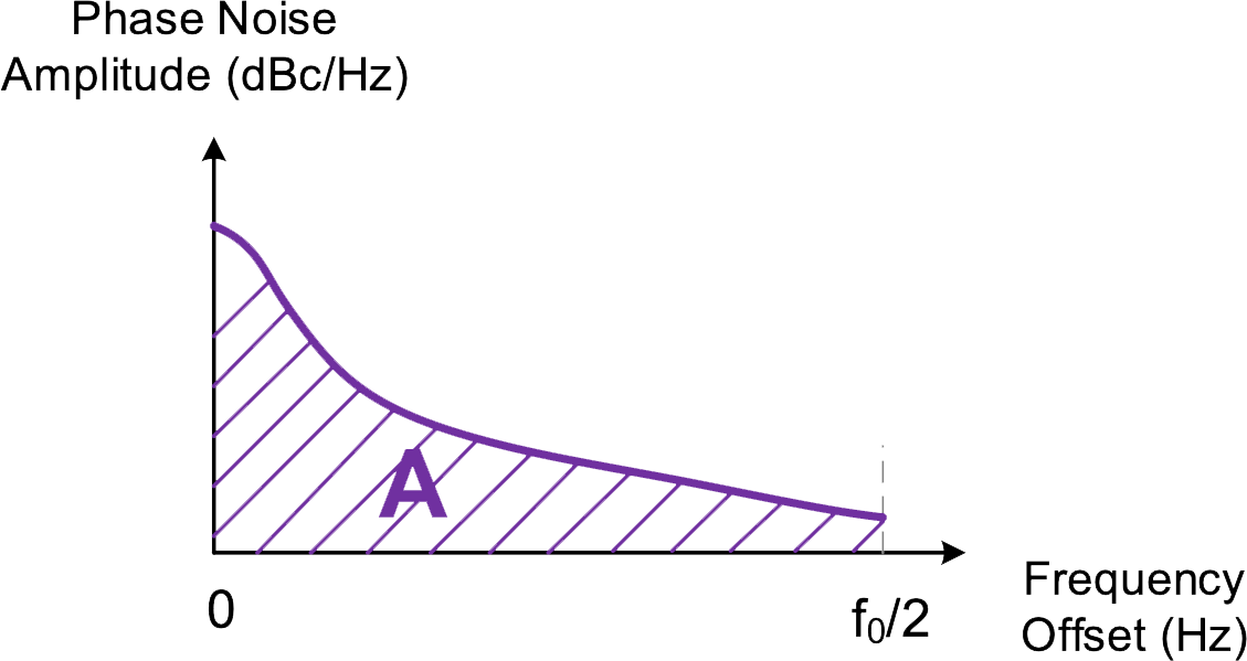
The area under the curve, A, is equal to the integrated phase noise power (dBc). The RMS absolute jitter value can be calculated from A, as shown in Equation 1.
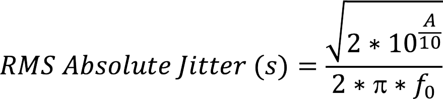
For systems that incorporate both digital and analog elements, converting phase noise to RMS absolute jitter can simplify the comparison between different clock sources.
Jitter and Phase Noise Impact on Audio Converters
The goal of an analog-to-digital converter (ADC) is to digitize an analog signal, without causing any degradation to the signal’s inherent signal-to-noise ratio (SNR).
Jitter on the converter clock couples into the signal during the sampling process introducing timing errors that modulate the input signal phase. This phase-noise modulation creates new distortion products. The spectral shape of the distortion products is dependent on the clock phase noise and the converter’s susceptibility to jitter across frequency.
The impact of the signal phase modulation, for certain phase noise shapes, can be observed as signal spread (a skirt-shaped effect in the frequency domain) and quantified by direct measurement of the signal distortion. Amplitude reduction of the fundamental tone (due to the signal spread) can, in some cases, also be observed and quantified through SNR measurements. Signal spread, and the resulting amplitude reduction of the fundamental tone, has a detrimental impact on perceived audio quality.
The impact of jitter (in the time domain) and signal phase modulation (in the frequency domain) is shown in Figure 3.
When designing a digital audio system, the performance of the ADC and the maximum tolerated level of jitter (along with other environmental performance disruptors) must be understood. The phase-noise analysis and understanding the ADC’s susceptibility to jitter across the audio frequency range is important when defining the jitter and phase noise requirements of the system.
Demonstrating the Impact of Jitter and Phase Noise
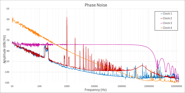
To demonstrate the potential impact of jitter and phase noise in a digital audio system, the phase noise of four clocks was characterized and the impact on the performance of an audio ADC was measured.
A description of the clocks is shown in Table 1.
| Clock | Description |
|---|---|
| 1 | Ideal reference clock generated by an instrumentation signal generator |
| 2 | Clock 1 with artificially added deterministic (tonal) 1 kHz jitter |
| 3 | Clock 1 with artificially added random jitter |
| 4 | Clock generated by a typical LCO |
The phase noise characteristics of Clock 1 – Clock 4 are shown in Figure 4. In this figure, the parameters for Clock 2 and Clock 3 are defined as Clock 2c and Clock 3c respectively in Table 2.
Degradation of the ADC Key Audio Performance Indicators
For each of the clocks described in Table 1, key ADC performance parameters (DNR and THD+N) were measured. For clocks 2 and 3, the absolute jitter amplitude was incremented with THD+N and DNR recorded for each increment (a – e). The tests were performed at a sampling rate of 48 kHz with a 1 VRMS, 1 kHz sine wave.
The results are shown in Table 2.
| RMS Absolute Jitter (ps) | ADC Performance | |||
|---|---|---|---|---|
| Clock | Baseband (100 Hz – 40 kHz) |
Wideband (100 Hz – f0/2) |
DNR (dB) (A-weighted) |
THD+N (dB) |
| 1 | 4.5 | 8 | 114.8 | –104.7 |
| 2a | 96 | 96 | 114.8 | –104.4 |
| 2b | 523 | 523 | 115 | –103.8 |
| 2c | 972 | 972 | 114.9 | –102.3 |
| 2d | 10000 | 10000 | 114.9 | –87.2 |
| 2e | 49000 | 49000 | 114.8 | –72.6 |
| 3a | 26 | 105 | 114.9 | –104.7 |
| 3b | 127 | 527 | 114.9 | –105.7 |
| 3c | 235 | 971 | 114.8 | –104.5 |
| 3d | 2400 | 10000 | 112.5 | –97.7 |
| 3e | 3000 | 12600 | 111.3 | –96.2 |
| 4 | 125 | 125 | 114.8 | –104.4 |
Notes:
-
DNR is defined as the ratio of spectral energy of the 1 kHz signal tone to the noise floor across the audio bandwidth.
-
THD+N is defined as the ratio of spectral energy of the 1 kHz signal to the integrated energy of the harmonics plus noise.
-
Highlighted values show more than 1 dB of degradation when compared to Clock 1. The 1 dB threshold was chosen to exclude differences attributable to measurement error.
ADC Output Signal Spectrum Analysis
Performance in a digital audio system can be degraded even if DNR and THD+N measurements do not indicate any issues. DNR and THD+N measurements do not capture all aspects of audio performance.
Further understanding of the impact of phase noise can be obtained through analysis of the output spectrum of the ADC when timed with different clocks.
The following observations were made for clocks 1, 2e, 3e, and 4, as described in Table 2.
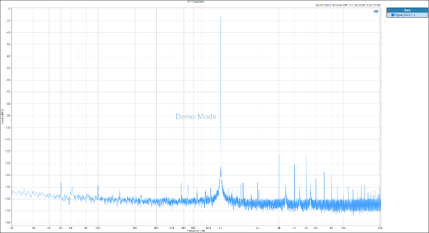
Observation 1: ADC Performance – Clock 1
Note that Clock 1 is a clock whose jitter does not impact the overall system performance.
The ADC performance against frequency within a controlled environment, with Clock 1 as the timing reference, is shown in Figure 5.
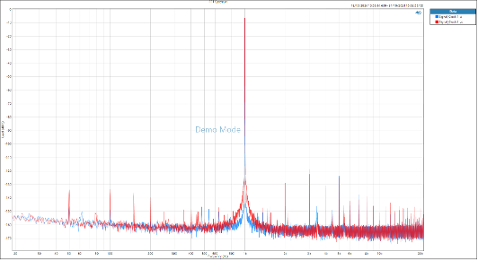
Observation 2. ADC Performance – Clock 2
Note that Clock 2 is Clock 1 with added deterministic (tonal) jitter.
The ADC performance against frequency, with Clock 2e as the timing reference, is shown in Figure 6. The performance with Clock 1 is shown for comparison.
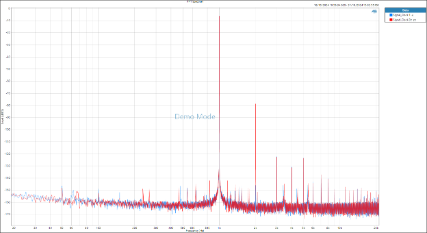
The spectrum shows that a prominent distortion spike manifests at 2 kHz. This is caused by the deterministic (tonal) jitter component of Clock 2e which degrades the THD component of THD+N. The spike frequency is dependent on the signal frequency and the jitter frequency.
Observation 3. ADC Performance – Clock 3
Note that Clock 3 is Clock 1 with added random jitter.
The ADC performance against frequency, with clock 3e as the timing reference, is shown in Figure 7. The performance with Clock 1 (in blue) is shown for comparison.
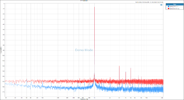
The spectrum shows an increase in the signal’s noise floor caused by the random jitter component of Clock 3e. Both DNR and THD+N measurements are degraded (as shown in Table 2) due to an increase of the noise component, N.
The absence of any prominent harmonic spike shows there is no significant degradation of the THD component resulting from random jitter.
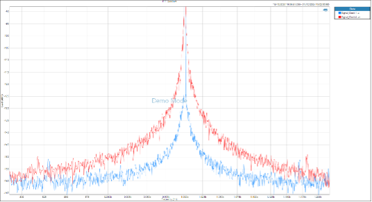
Observation 4. ADC Performance – Clock 4
Note that Clock 4 is a clock generated by an LC oscillator.
The ADC performance against frequency, with Clock 4 as the timing reference, is shown in Figure 8. The performance with Clock 1 (in blue) is shown for comparison.
Clocks with low-frequency phase noise cause phase modulation of the 1 kHz signal tone (observed as tonal spread). A magnified view of the tonal spread is shown in Figure 9.
The tonal spread is caused by the low-frequency phase noise present in Clock 4. However, as shown in Table 2, THD+N and DNR have less than 1 dB of degradation. The phase modulation could have been missed if a spectrum analysis was not performed.
Conclusion
In conclusion, jitter and phase noise can affect the overall performance of a digital audio system. The impact of the clock signal quality can be observed by analyzing the audio key performance indicators and the spectrum of the output signal. Understanding the impact of jitter and phase noise in the system performance enables the designer to understand the clock requirements.
Cirrus Logic’s series of timing devices, make system level clocking easy. Providing you with a reliable heartbeat for your audio system.
Perception is Subjective
In most cases, the consumers of digitized audio signals are humans listening to music in their home, while commuting, or working. Can humans perceive the artifacts of degradation caused by a low-quality clock? How do they affect the listener’s perceived acoustic experience?
1 AES-12id-2020, “Digital Audio Measurements – Jitter performance specifications” (2020), Audio Engineering Society.
